Wednesday, August 6, 2025
Home Blog Page 22

Spirent Communications Unveils New 5G Fixed Wireless Access (FWA) Testing Services

0

Spirent Communications, a leading provider of test and assurance solutions for next-generation devices and networks, has announced the launch of its 5G Fixed Wireless Access (FWA) testing services. These solutions are designed to offer comprehensive lab-based 5G/Wi-Fi gateway testing and live network competitive benchmarking, enabling communications service providers (CSPs) and device manufacturers to optimize quality of experience (QoE) and stand out in a competitive market.

With the rapid acceleration of 5G FWA adoption, there is a growing need for thorough network performance evaluations. Over 200 CSPs have already introduced home services, while 20 CSPs have launched 5G FWA business offerings. Spirent’s new 5G FWA services address this demand by providing advanced testing solutions that deliver key insights into user experience, allowing operators to enhance customer satisfaction and drive revenue growth.

5G FWA represents a significant opportunity for CSPs to expand their revenue streams,” said Stephen Douglas, Head of Market Strategy at Spirent. “Maximizing its potential requires prioritizing user experience testing, which is exactly what our new solutions deliver. These services can also help save providers, device manufacturers, and network vendors millions in troubleshooting costs by identifying issues earlier in the development process.”

Spirent’s 5G FWA solutions leverage the company’s proven methodologies and global cloud-based measurement systems to help service providers and vendors optimize services for superior QoE. They also offer confidential and reliable competitive benchmarking to validate performance claims. These new services are part of Spirent’s ongoing efforts to help customers swiftly launch, optimize, and monetize 5G networks.

Spirent’s 5G FWA services offer insights through detailed testing across various user scenarios, including:

  • General data and web browsing
  • VoWiFi (Voice over Wi-Fi)
  • Video streaming QoE
  • Cloud gaming QoE
  • RF environment characterization

By conducting these tests, CSPs gain a deeper understanding of their FWA service performance in comparison to others in the market. Spirent’s tailored benchmark testing provides real-world data to highlight areas for optimization, helping CSPs enhance customer satisfaction, improve operational efficiency, reduce costs, and optimize their infrastructure to better serve users during peak and off-peak times.

For more information, visit www.spirent.com.

STMicroelectronics to Announce Q3 2024 Earnings on October 31 and Host Capital Markets Day in November

STMicroelectronics, a global leader in semiconductor technology, has announced that it will release its third-quarter 2024 earnings prior to the opening of trading on the European Stock Exchanges on October 31, 2024. The earnings report will be made available immediately after its release on the company’s official website, www.st.com.

Following the release, STMicroelectronics will host a conference call for analysts, investors, and reporters to discuss the Q3 2024 financial results and provide an update on the company’s current business outlook. The call will take place on October 31, 2024, at 9:30 a.m. Central European Time (CET) / 3:30 a.m. U.S. Eastern Time (ET).

A live webcast of the conference call, available in listen-only mode, will be accessible via ST’s investor relations website at https://investors.st.com. The webcast will remain available for replay until November 15, 2024.

Additionally, STMicroelectronics will host its 2024 Capital Markets Day on November 20, 2024, from 9:00 a.m. to 1:15 p.m. Central European Time (CET) / 3:00 a.m. to 7:15 a.m. U.S. Eastern Time (ET) in Paris, France. The event will feature a live webcast with video, audio, and presentation slides, accessible at https://investors.st.com. Presentations and a recording of the event will be made available on the same website after the event.

For more information, visit www.st.com.

Amkor Technology and TSMC Collaborate to Expand Advanced Packaging and Test Capabilities in Arizona

0

Amkor Technology and TSMC have signed a memorandum of understanding to collaborate on bringing advanced packaging and testing capabilities to Arizona, enhancing the region’s semiconductor ecosystem. This agreement builds on the longstanding partnership between the two companies in delivering high-volume, cutting-edge technologies for semiconductor packaging and testing, targeting critical markets such as high-performance computing and communications.

As part of the agreement, TSMC will contract Amkor to provide turnkey advanced packaging and test services at Amkor’s upcoming facility in Peoria, Arizona. These services will support TSMC’s customers, especially those utilizing TSMC’s advanced wafer fabrication facilities in Phoenix. By having TSMC’s front-end fabrication and Amkor’s back-end services located in close proximity, the partnership will accelerate overall product cycle times and improve efficiency.

Both companies will collaborate to define specific packaging technologies, including TSMC’s Integrated Fan-Out (InFO) and Chip on Wafer on Substrate (CoWoS), to meet the needs of mutual customers.

This partnership highlights the shared commitment to providing geographic flexibility in semiconductor manufacturing, fostering a comprehensive semiconductor ecosystem in the U.S., and aligning technology seamlessly across the global supply chain.

Giel Rutten, President and CEO of Amkor, said,
“Amkor is proud to collaborate with TSMC to integrate silicon manufacturing and packaging processes through an efficient turnkey model in the U.S. This partnership underscores our commitment to innovation and advancing semiconductor technology while ensuring resilient supply chains.”

Dr. Kevin Zhang, TSMC’s Senior Vice President of Business Development and Global Sales, added,
“As our customers increasingly depend on advanced packaging technologies for breakthroughs in mobile applications, AI, and high-performance computing, we are pleased to collaborate with our trusted partner Amkor. Together, we will support a more diverse manufacturing footprint and maximize the value of our Phoenix fabs.”

For more information about Amkor’s Arizona operations, visit Amkor Technology.

Autonomous Driving and Edge AI: Imagimob and Infineon Team Up to Enhance Automotive Machine Learning

0

Autonomous and automated driving, along with electrification, is a key trend in the automotive industry. Artificial Intelligence (AI) plays a crucial role in this transformation, enabling vehicles to perform tasks such as detecting pedestrians, analyzing driver behavior, recognizing traffic signs, and controlling trajectories. Edge AI is a critical component in this trend, as autonomous driving demands AI systems with robust machine learning capabilities and processors that can handle vast amounts of data in real-time, safely and securely.

Autonomous Driving and Edge AI: Imagimob and Infineon Team Up to Enhance Automotive Machine Learning

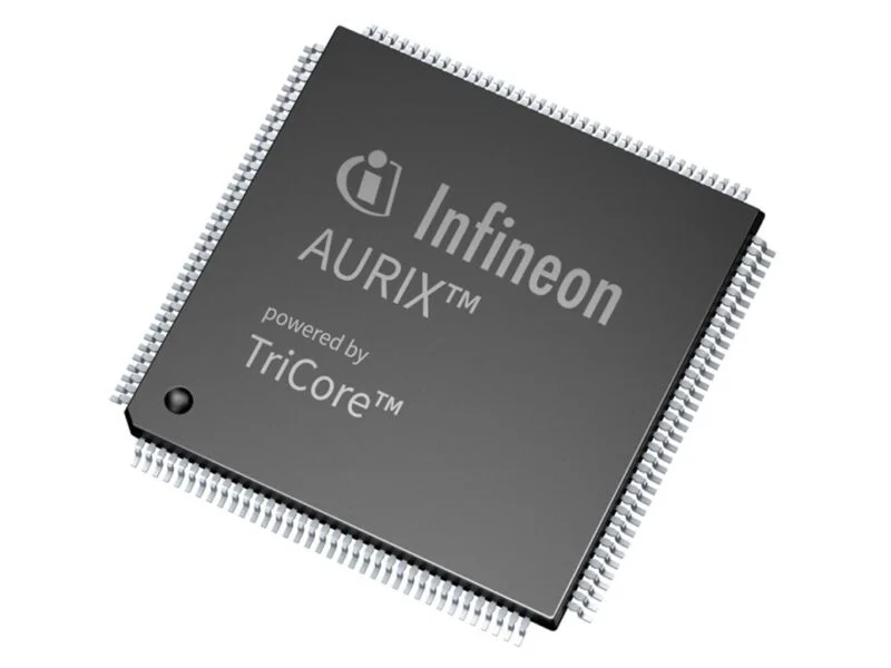
To meet this challenge, Imagimob, a company under Infineon Technologies AG, has strengthened its automotive machine learning portfolio by integrating machine learning (ML) capabilities into Infineon’s Automotive ASIL-D compliant microcontrollers (MCUs), such as the AURIX TC3x and AURIX TC4x families.

Thomas Boehm, Senior Vice President of Microcontrollers at Infineon, emphasized the importance of this development, stating,
“Integrating secure and reliable AI capabilities into microcontroller families is essential for the advancement of autonomous driving applications in the automotive sector. We are proud that our AURIX microcontrollers are now supported by Imagimob Studio, which makes them accessible to developers worldwide and solidifies our position as a leading innovator in the industry.”

Alexander Samuelsson, CTO of Imagimob, highlighted the platform’s versatility, noting,
“With the integration of AURIX into Imagimob Studio, we are bringing full machine learning capabilities to the automotive sector. This means all the use cases we support are now available for Infineon’s AURIX microcontrollers.”

With Imagimob Studio, developers can now create and deploy robust machine learning models for Edge AI on Infineon’s proven AURIX MCUs. The process starts with model creation in Imagimob Studio, after which users can easily deploy the model to the MCUs. The platform simplifies the entire process by providing step-by-step guidance, enabling developers to implement sophisticated ML models on MCUs with ease.

Additionally, Imagimob Studio includes a sample project for siren detection, showcasing the process of creating and deploying a model. This example allows users to explore how to build acoustic models using AURIX MCUs and a microphone shield. Imagimob has also developed regression models to calculate metrics like remaining battery power, health status, and usage time.

Advanced AI Use Cases with AURIX TC4x

The AURIX TC4x family of MCUs offers a seamless upgrade path from the AURIX TC3x series, providing enhanced performance thanks to its next-generation TriCore™ 1.8 architecture. The TC4x family also features a scalable accelerator suite, including a parallel processing unit (PPU) and multiple intelligent accelerators, enabling cost-effective AI integration.

These advancements in the AURIX TC4x series allow developers to deploy multiple or more complex machine learning models. For example, while the AURIX TC3x can manage basic tasks like siren detection, the AURIX TC4x can handle both siren detection and voice interaction simultaneously, showcasing its ability to support more advanced AI use cases.

Availability

Imagimob Studio is available at https://www.imagimob.com/studio, and further details about Infineon’s AURIX family of microcontrollers can be found at http://www.infineon.com/AURIX.

OMNIVISION Unveils Industry-First 3MP OX03H10 Automotive Image Sensor with TheiaCel Technology at AutoSens Europe 2024

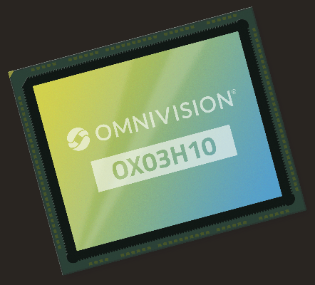
OMNIVISION, a global leader in semiconductor solutions specializing in advanced digital imaging, analog, and touch & display technology, has introduced the OX03H10 CMOS image sensor. This new 3-megapixel (MP) sensor, featuring 3.0-micron (µm) pixels, is the first and only automotive viewing sensor to incorporate TheiaCel technology. Announced at AutoSens Europe 2024, the OX03H10 is designed to enhance driving safety by providing exceptional image clarity in all lighting conditions, making it ideal for surround-view and rear-view cameras.

OMNIVISION Unveils Industry-First 3MP OX03H10 Automotive Image Sensor with TheiaCel Technology at AutoSens Europe 2024

Naresh Shetty, automotive product marketing manager at OMNIVISION, explained,
“The OX03H10 delivers outstanding low-light performance and unmatched LED flicker mitigation (LFM) by using a single exposure to capture a 140 dB dynamic range. This is made possible through our TheiaCel technology, which combines lateral overflow integration capacitor (LOFIC) technology with OMNIVISION’s single-exposure DCG and split-pixel high dynamic range (HDR) technology, ensuring top-tier image quality in any lighting environment. We are thrilled to introduce the OX03H10 for next-generation automotive cameras, improving visibility and safety for drivers.”

The OX03H10 offers 1920 x 1536 resolution at 60 frames per second (fps) while maintaining low power consumption. Its 3.0-µm pixel design, based on PureCel Plus-S stacking technology, delivers the smallest pixel and highest resolution in a 1/2.44-inch optical format. The sensor also comes in a compact a-CSP package and is pin-to-pin compatible with OMNIVISION’s OX03F10 sensor, enabling seamless upgrades. Additionally, the OX03H10 meets ASIL-C functional safety standards, offers cybersecurity features, and supports a MIPI output interface.

The OX03H10 is available for sampling now, with mass production expected in the first half of 2025. For more information, visit OMNIVISION at AutoSens Europe 2024, Booth 300, or contact an OMNIVISION sales representative at www.ovt.com/contact-sales.

Livguard Launches High-Frequency Solar Inverters at 17th Renewable Energy India Expo 2024

0

Livguard, a leading brand under the SAR Group, has introduced its latest range of High-Frequency Solar Inverters at the 17th Renewable Energy India (REI) Expo 2024, held at the India Expo Center in Greater Noida on October 3rd, 2024. The launch event was led by Mr. Alankar Mittal, President and Business Unit Head of Solar & Exports at Livguard.

The new product lineup includes the Hybrid Series and Off-Grid Series inverters, both of which utilize transformer-less technology to offer enhanced efficiency and reliability. These inverters are compatible with both Lead Acid and Lithium Batteries, and come equipped with built-in Wi-Fi, enabling users to monitor performance conveniently via smartphones. Additionally, the inverters feature UPS functionality, ensuring uninterrupted power supply for PCs and household appliances. Alongside the inverters, Livguard also launched other innovative products, such as lithium-based ESS, high-efficiency Bi-facial panels, and high-efficiency DCR panels.

These new offerings complement Livguard’s existing range of solar solutions, which cater to the needs of residential and small business sectors. Livguard also offers consumer finance options for solar investments, ranging from 1 lakh to 2 crore rupees, and provides interest-free loans on their off-grid and hybrid solutions for up to six months.

Livguard’s solar product portfolio, including Off-Grid, On-Grid, Hybrid solutions, and Lithium ESS, offers flexibility in battery and grid operations, delivering higher ROI and uninterrupted solar energy for both savings and backup purposes. The Livmonitor 360 app allows users to monitor solar energy generation with a single click. Livguard also provides a PAN India service team of over 1,000 members, along with on-call assistance from solar experts, ensuring top-tier installation quality and customer satisfaction.

The REI Expo, Asia’s leading B2B platform for renewable energy, attracted over 800 exhibitors and 40,000 visitors, including industry experts and professionals.

Mr. Alankar Mittal, President Business Unit Head of Solar & International Business at Livguard, expressed his enthusiasm about the launch, stating,
“Livguard Solar and Livfast Solar continue to pave the way for innovations that are reshaping India’s energy landscape. The REI Expo provided the perfect platform to showcase our advanced solutions, reinforcing our commitment to a greener future. We are thrilled by the response to our High-Frequency Solar Inverters, which are compact, lightweight, RMS-enabled, offer quick changeover, and operate with low noise. We see enormous potential in India’s renewable energy sector and will remain at the forefront of developing innovative products that drive sustainable energy solutions in India.”

Livguard Solar continues to be a trusted name in the renewable energy sector, offering certified solutions and smart monitoring systems that provide efficient, clean energy for homes and businesses. The brand is dedicated to enhancing energy security, sustainability, and innovation in both India and the global market. Livguard aligns its mission with the Government of India’s vision for the renewable energy sector, contributing to the country’s ongoing energy transformation.

OMNIVISION Unveils OX12A10 12MP CMOS Image Sensor with TheiaCel Technology at AutoSens Europe 2024

0

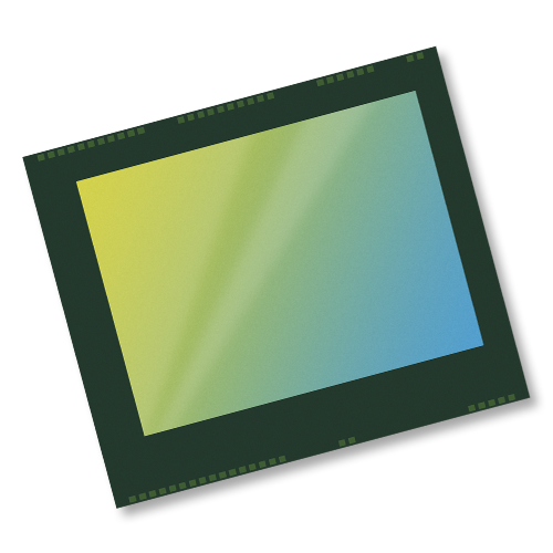
OMNIVISION, a global leader in semiconductor solutions specializing in advanced digital imaging, analog, and touch & display technologies, has introduced its OX12A10 12-megapixel (MP) CMOS image sensor featuring TheiaCel technology at AutoSens Europe 2024. This new sensor enhances automotive safety by delivering superior resolution and image quality under all lighting conditions, making it ideal for high-performance front machine vision cameras used in Advanced Driver Assistance Systems (ADAS) and autonomous driving (AD) applications.

OMNIVISION Unveils OX12A10 12MP CMOS Image Sensor with TheiaCel Technology at AutoSens Europe 2024

The OX12A10 sensor, offering 12MP resolution, is the highest-resolution device in OMNIVISION’s 2.1-micron (µm) TheiaCel product line, which also includes the 8MP OX08D10 and 5MP OX05D10 sensors. The TheiaCel technology utilizes next-generation lateral overflow integration capacitors (LOFIC) and OMNIVISION’s dual conversion gain (DCG) high dynamic range (HDR) technology to eliminate LED flicker and ensure consistent image quality across various lighting environments. TheiaCel also provides a broader dynamic range compared to earlier automotive HDR systems.

Dr. Paul Wu, head of automotive product marketing at OMNIVISION, commented, “Our sensing solutions are designed to enhance driving safety and autonomy. The OX12A10 combines high resolution, excellent low-light performance, LED flicker mitigation (LFM), compact size, power efficiency, and superior high-temperature performance in one device. TheiaCel technology, introduced at AutoSens last year, has generated significant interest, and we’re excited to expand the family with the first high-performance 12MP sensor for the automotive industry. Our 5MP and 8MP solutions cater to mainstream vehicles, while the OX12A10 targets next-gen ADAS and AD vision systems.”

With a 1/1.43-inch optical format, the OX12A10 is the first sensor to feature OMNIVISION’s a-CSP+ package technology. Its compact design, measuring just 12450µm x 8100µm, is more space-efficient than traditional ball grid array (BGA) packages.

The OX12A10 is available for sampling now, with mass production scheduled for Q3 2025. For further details, visit OMNIVISION’s booth at AutoSens Europe 2024, Booth 300, from October 8-10, 2024, in Barcelona, Spain, or contact an OMNIVISION sales representative at www.ovt.com/contact-sales.

Global Gamification Mobile Application in Healthcare Market Set to Reach $4.48 Billion by 2024, Driven by Rising Chronic Disease Prevalence

0

Global Gamification Mobile Application: According to Fact.MR, a leading provider of market research and competitive intelligence, the global gamification mobile application in healthcare market is projected to reach a valuation of US$ 4.48 billion by 2024, with an impressive CAGR of 21.4% expected from 2024 to 2034. The growing prevalence of chronic conditions like cardiovascular diseases, cancer, obesity, and diabetes is a significant factor driving the demand for gamified healthcare apps.

A report from the OECD indicates that over one-third of adults globally suffer from long-term illnesses, with 43% of the low-income population diagnosed with chronic diseases. The cost and prevalence of these conditions are expected to rise sharply in the coming years. In fact, “The Burden of Chronic Disease” report projects that by 2030, the global cost of managing chronic illnesses will exceed US$ 47 trillion.

The adoption of gamification in healthcare, along with its growing role in education, has spurred market growth. Additionally, the integration of AI and machine learning into wearable and handheld devices has accelerated the expansion of gamified healthcare applications, enhancing their effectiveness and appeal.

Key Insights from the Market Study:

  • The global gamification mobile application in healthcare market is forecasted to grow at a CAGR of 21.4% and is expected to reach US$ 31.17 billion by 2034.
  • Between 2019 and 2023, the market created an opportunity worth US$ 1.69 billion, growing at a CAGR of 11.9%.
  • Leading companies in the market include Mango Health, Propeller Health, Omada Health Inc., Fitbit Health Solutions, Akili, Inc., and other emerging startups.
  • The exercise games segment is estimated to grow at a CAGR of 22.7% between 2024 and 2034.

Growing Demand for Gamified Healthcare Solutions

According to a Fact.MR analyst, the increasing penetration of smartphones, AI technologies, and interactive patient engagement solutions in the healthcare sector is driving demand for gamified mobile health apps. The growing interest in gamified solutions to encourage engagement across various demographics, particularly the aging population, has been fueling market growth. Collaborative strategies and partnerships among major players have also significantly boosted market expansion. Leading companies are investing in R&D in communication technologies and mobile computing, resulting in promising improvements in physical activity (PA) and behavior change interventions.

Recent Industry Developments in Gamified Healthcare Applications

In June 2023, UC Davis Health and Propeller Health announced a collaboration to offer personalized treatment for high-risk patients with asthma and chronic obstructive pulmonary disease (COPD), aiming to improve health outcomes. The use of gamification design elements such as progress bars, leaderboards, and points has strengthened engagement between consumers and healthcare apps, leading to better patient adherence and outcomes.

Moreover, the GSMA 2023 report highlights the potential of 5G standalone and 5G Advanced technologies, which will increase investments in digital healthcare solutions. By 2030, the penetration rate of mobile internet users is expected to rise to 68%, from 58% in 2023, creating wide opportunities for growth in the gamification healthcare market.

Key Market Players Leading Innovation

Notable companies driving innovation in this space include Mango Health, Propeller Health, Omada Health Inc., Fitbit Health Solutions, Akili, Inc., Calm.com, Inc., Headspace Inc., Sleep Cycle, and Lumi Health (Apple Inc.). These companies continue to develop new and advanced gamified mobile applications to meet the evolving needs of the healthcare industry.

Conclusion

The global gamification mobile application in healthcare market is poised for significant growth, with increasing demand for personalized, engaging, and effective healthcare solutions. Technological advancements, rising smartphone penetration, and the adoption of AI and machine learning will play crucial roles in shaping the future of this market. As more companies invest in innovative solutions, gamification in healthcare is set to transform patient engagement, physical activity, and chronic disease management.

Fact.MR provides further valuable insights in its latest report, which covers historical data from 2019 to 2023 and forecasts from 2024 to 2034, offering a detailed analysis of product types, applications, and key regions globally. Click here

The Next Leap in Semiconductors: The 1.4nm Process Node

0

As the semiconductor industry moves towards the 1.4nm process node, expected to launch in 2027, it signifies a major technological milestone in miniaturization and efficiency. While the 2nm node is still on the horizon for 2025, the industry is already preparing for the next phase, where advancements in transistor density, energy efficiency, and performance will redefine the limits of computing power.

Pushing the Boundaries with 1.4nm Technology

The 1.4nm process node will unlock new possibilities for fields such as artificial intelligence (AI) and quantum computing. Designers are not just working to reduce the size of electronic components; they are pushing the boundaries of technology itself. These advancements, aligned with Moore’s Law, aim to meet growing demands for more efficient and powerful computing systems.

The development of this process node relies heavily on cutting-edge manufacturing technology, such as Extreme Ultraviolet (EUV) lithography. Developed by ASML, these machines, valued at around $400 million, are essential for the precision needed to produce chips at such small scales. As we look toward 2027, the evolution of semiconductor technology will have profound implications for the industry and beyond.

The Role of EUV Lithography in Miniaturization

EUV lithography is the key technology driving miniaturization in semiconductor manufacturing. It uses shorter wavelengths of light compared to traditional methods, allowing for more precise etching of patterns onto silicon wafers. This technique enables companies to fit billions of transistors onto a single chip, which was a significant challenge using older Deep Ultraviolet (DUV) lithography.

Major industry players, like Intel, are already investing heavily in High-NA EUV lithography machines from ASML to stay ahead in the race for 1.4nm technology. These machines are central to Intel’s strategy to advance its chip manufacturing capabilities.

The Evolution of Transistor Density

From the creation of the integrated circuit in the 1950s, which housed just a few transistors, the industry has evolved to create chips containing billions of transistors. The shift from microscale to nanoscale technology has brought immense improvements in computing power, efficiency, and complexity.

Transitioning to the 1.4nm node will represent the most significant leap in transistor density and performance to date. This evolution, however, presents new challenges in materials science and fabrication techniques. The industry will need to innovate further in lithography and explore new materials capable of managing heat and behavior at quantum scales.

Rather than focusing solely on the number of transistors per unit, we are moving toward a focus on transistors per 3D volume, which is crucial for advanced applications such as virtual reality (VR), augmented reality (AR), and autonomous vehicles.

Intel’s Role in Advancing 1.4nm Technology

Currently, Intel uses EUV technology in three of its fabrication plants—Intel 4, Intel 3, and Intel 20A. While DUV lithography is still dominant in Intel’s Intel 7 process, the company anticipates a major shift toward EUV-based nodes in the near future. Intel’s focus is not just on advancing lithography but also on expanding its manufacturing capacity and investing in advanced packaging techniques.

Beyond the 1.4nm Node

Looking beyond the 1.4nm node, the industry faces the physical and technical limits of silicon-based technology. As process nodes shrink further, challenges like quantum tunneling and heat dissipation become more significant, potentially affecting chip efficiency and reliability.

The search for alternative materials is already underway. Emerging technologies like graphene and transition metal dichalcogenides offer promising electrical, thermal, and mechanical properties at atomic thicknesses. Quantum dots also show potential for advancing photonics and quantum computing, providing new ways to process and store information. Additionally, 3D integrated circuit (IC) packaging offers a solution to enhance performance by stacking multiple chiplets or dies into a single package.

The Impact of 1.4nm and Beyond

Advancing beyond the 1.4nm node opens up a new world of possibilities. AI systems will become more powerful and efficient, capable of complex reasoning while consuming less energy. Quantum computing, benefiting from advancements in quantum materials and quantum dots, will become more practical, solving problems that are difficult for classical computers.

The continuous push for miniaturization will redefine the future of computing, offering breakthroughs in energy efficiency and processing power.

Conclusion

The journey toward and beyond the 1.4nm node is not just about shrinking electronics but about redefining the architecture of computing technology. As we approach 2027, this milestone promises to revolutionize industries like AI and quantum computing, bringing unparalleled efficiency and performance. With companies like Intel investing in EUV lithography and advanced packaging, the semiconductor industry is set for a significant transformation, driving the future of computing into new and exciting realms.

For more information, visit: https://www.mouser.in/blog/next-leap-in-semiconductors.

Vertiv Wins Three Awards at 18th Data Center Summit and Awards 2024

0

Vertiv, a global leader in critical digital infrastructure and continuity solutions, secured three prestigious awards at the 18th Data Center Summit and Awards 2024 held at The Lalit, Mumbai. The event, attended by industry experts such as CXOs, CTOs, VPs, and IT directors, provided Vertiv with an opportunity to highlight its innovative solutions addressing the evolving demands of modern data centers.

Vertiv received the following accolades:

  • Sustainable Power Management Solutions of the Year 2023 – Power Management (Energy Efficient Management)
  • AI Future-ready Data Center Cooling Award for Design and Innovation 2023 – Cooling (Energy Efficient Management)
  • Leading Contributor in Future-ready AI Data Centers – Data Center

During the summit, Vertiv also introduced its Vertiv SmartRow solution through an immersive experience using the Vertiv XR App ecosystem, offering attendees a virtual demonstration of the company’s cutting-edge products and continuity solutions.

The Data Center Summit featured presentations from industry leaders on the latest trends and innovations in the data center sector, along with exhibits and one-on-one discussions with partner sponsors. Reflecting on the awards, Dr. AS Prasad, Vice President – Product Management at Vertiv, stated:
“We are honored to receive these prestigious awards, which highlight Vertiv’s ongoing commitment to innovation in the data center industry. As our customers’ needs grow more sophisticated, we remain dedicated to delivering advanced, eco-friendly solutions that meet their evolving requirements. We look forward to continuing this journey of innovation, collaboration, and excellence as we navigate the ever-changing data center landscape.”