Saturday, August 2, 2025
Home Blog Page 17

Viavi Solutions Partners with Telefónica HISPAM to Deliver Automated Network Inventory Management with NITRO AIOps

0

Viavi Solutions Inc. has announced a new collaboration with Telefónica Hispanoamérica (HISPAM) to provide automated network inventory management using the advanced VIAVI NITRO AIOps platform. This partnership will enhance Telefónica HISPAM’s operations across its regions, including Argentina, Chile, Colombia, Ecuador, Peru, Mexico, Uruguay, and Venezuela.

The NITRO AIOps solution will manage both passive and active network components, covering various network domains such as Radio, Core, IP, Transmission, Microwave, and Fiber Optics. Additionally, the platform will include IP Address Management (IPAM) capabilities to streamline operations. The system is designed to auto-discover and catalog physical, software, and virtual assets, as well as their connections, ensuring full visibility of Telefónica HISPAM’s network infrastructure.


Driving Innovation in Network Management

Gabriel Rodriguez, Head of OSS Systems at Telefónica HISPAM, emphasized the importance of this partnership:
“Telefónica HISPAM is focused on building a modern, efficient OSS architecture, and VIAVI’s AIOps solution plays a key role in that mission. With their proven tools and expertise, we are better equipped to manage our expanding regional networks and continue delivering reliable services to our subscribers.”

VIAVI’s NITRO AIOps platform integrates network assurance and inventory management, providing a unified, end-to-end view of all resources and services through a single interface. The system is designed to manage multi-vendor, multi-technology, and multi-domain networks, delivering real-time network insights through AI/ML-based analytics. Patented topology algorithms further enhance network reliability, ensuring consistent performance across all infrastructure layers.


Key Benefits of the NITRO AIOps Platform

  1. Comprehensive Network Visibility: Brings all network data sources together under a single interface, offering a holistic view of operations.
  2. Proactive Issue Detection: Identifies and resolves potential problems before they impact users, reducing downtime and improving service reliability.
  3. AI-Driven Analytics: Assists with capacity planning, predictive maintenance, and anomaly detection, helping operators manage resources efficiently.
  4. Real-Time Situational Awareness: Enables network teams to monitor and respond to network changes instantly, ensuring seamless performance.

Improving Service Quality with AI-Powered Solutions

Deepak Shahane, Senior Vice President and General Manager of Service Enablement at VIAVI, highlighted the impact of the collaboration:
“We are excited to partner with Telefónica HISPAM to demonstrate the power of NITRO AIOps. With our automated tools, we aim to detect and address complex network issues before they escalate, leading to faster resolutions and minimizing the impact on users. Our platform meets Telefónica HISPAM’s real-time needs, offering comprehensive network visibility and operational control.”


Optimizing Operations and Reducing Costs

With proactive monitoring, NITRO AIOps helps Telefónica HISPAM identify bottlenecks and performance anomalies before they affect service quality. This ensures seamless operations while reducing downtime and disruptions. Additionally, the platform’s predictive maintenance capabilities contribute to cost savings by reducing the frequency of network failures and improving overall operational efficiency.

AI-based analytics also support capacity planning and resource optimization, ensuring that the network continues to meet evolving demands. This holistic approach allows Telefónica HISPAM to maintain high service quality while controlling operational costs and minimizing network risks.


Conclusion

The partnership between Viavi Solutions and Telefónica HISPAM is set to transform how the telecommunications provider manages its regional networks. With NITRO AIOps, Telefónica HISPAM will benefit from proactive monitoring, predictive analytics, and seamless network management, ensuring the delivery of reliable, high-quality services to its subscribers.

For more information about Viavi Solutions and its offerings, visit www.viavisolutions.com.

Microchip Introduces PIC64HX Microprocessors for Intelligent Edge Applications

The global edge computing market is expected to grow by more than 30% over the next five years, driven by demand from industries such as aerospace, defense, medical, and industrial sectors. In response to this need for high-performance solutions in mixed-criticality systems, Microchip Technology has unveiled the PIC64HX family of microprocessors (MPUs). Unlike conventional MPUs, the PIC64HX series is specifically designed to address the challenges of intelligent edge computing applications.


High-Performance RISC-V MPUs for Advanced AI/ML Applications

The PIC64HX is the latest addition to Microchip’s 64-bit microprocessor portfolio. These multicore RISC-V MPUs offer advanced capabilities for Artificial Intelligence (AI) and Machine Learning (ML) workloads, along with Time-Sensitive Networking (TSN) Ethernet capabilities for seamless real-time data communication. The processors are also equipped with post-quantum cryptography, providing defense-grade security designed to meet future threats posed by quantum computing.

These MPUs are engineered to ensure fault tolerance, scalability, resiliency, and power efficiency, making them ideal for mission-critical applications in aerospace, automotive, and industrial automation.


Integrating Networking and Compute for System Efficiency

According to Maher Fahmi, corporate vice president at Microchip, the PIC64HX MPU brings together advanced networking and compute capabilities, simplifying system designs and lowering development costs. “By embedding TSN Ethernet switching directly into the MPU, we enable developers to align standards-based networking with compute operations, reducing time-to-market and increasing design efficiency,” said Fahmi.

The integrated TSN Ethernet switch supports key emerging standards:

  • IEEE P802.1DP: TSN for aerospace onboard communications
  • IEEE P802.1DG: TSN for in-vehicle automotive networks
  • IEEE/IEC 60802: TSN profile for industrial automation

These features provide reliable, low-latency communication across different industry sectors.


Empowering Intelligent Edge with Versatile Compute Options

The PIC64HX features eight SiFive Intelligence X280 cores, designed for vector processing and high-performance AI workloads. These cores offer flexibility by supporting different configurations:

  • Symmetric Multiprocessing (SMP)
  • Asymmetric Multiprocessing (AMP)
  • Dual-core lockstep mode for enhanced fault tolerance

The architecture also includes WorldGuard hardware-based partitioning, enabling secure isolation for different tasks, which is critical in applications where mixed-criticality systems must run side-by-side safely.


Aviation Industry Sees Potential in RISC-V Technology

The OHPERA Consortium, a coalition of aerospace companies working toward next-generation aviation technologies, recognizes the potential of RISC-V processors. According to Christophe Vlacich, OHPERA’s technical leader, modern aircraft require advanced processors for flight control, cabin networking, engine control, and cockpit displays. “We are excited about the capabilities of Microchip’s PIC64HX MPUs, which meet the performance, security, and networking demands of future aviation systems,” Vlacich noted.


Addressing Future Security Threats with Post-Quantum Cryptography

The rise of quantum computing presents new challenges to existing cybersecurity systems, as many current encryption methods will become vulnerable. In preparation for this shift, the PIC64HX MPUs integrate NIST-approved post-quantum cryptographic algorithms, including:

  • FIPS 203 (ML-KEM): Key encapsulation mechanism
  • FIPS 204 (ML-DSA): Digital signature algorithm

These algorithms offer enhanced protection for sensitive systems, aligning with evolving security requirements across industries.


Comprehensive Development Tools and Ecosystem Support

Microchip provides a robust suite of development tools to support the PIC64HX MPU family. This includes libraries, drivers, and boot firmware, with support for both open-source and commercial operating systems like Linux and RTEMS, as well as hypervisors such as Xen.

The MPUs leverage Microchip’s Mi-V ecosystem, which offers a wide range of tools and resources to accelerate RISC-V development efforts. To further simplify design, Microchip offers the Curiosity Ultra+ evaluation kit and has partnered with Aries Embedded to create System-on-Modules (SoMs) for mission-critical edge applications.

Andreas Widder, CEO of Aries Embedded, emphasized the value of this collaboration: “As a committed supporter of the RISC-V ecosystem, we are excited to partner with Microchip to bring the PIC64HX to market and support innovative edge solutions.”


Availability and Early Access

Microchip plans to provide PIC64HX MPU samples to its early access partners starting in 2025. For more details or to connect with a Microchip sales representative, please visit Microchip’s official website.


Conclusion: Shaping the Future of Edge Computing

With its blend of high-performance computing, real-time networking, and defense-grade security, the PIC64HX MPU positions Microchip as a leader in the growing edge computing market. The processor’s ability to meet the demands of AI-driven intelligent systems while ensuring security and fault tolerance makes it a valuable solution for industries such as aerospace, automotive, and industrial automation. As edge computing becomes increasingly essential, the PIC64HX MPU family offers a future-ready platform to power the next wave of mission-critical applications.

Anritsu and Bluetest Introduce Advanced OTA Measurement Solution for 2×2 MIMO Testing in IEEE 802.11be WLAN Devices

Anritsu and Bluetest have combined their latest product innovations to offer a comprehensive Over-the-Air (OTA) measurement solution for testing RF performance in a 2×2 MIMO environment, supporting the tri-frequency bands defined by the newest WLAN standard, IEEE 802.11be.

This collaboration focuses on accurately measuring transmit power (Total Radiated Power, TRP) and receiver sensitivity (Total Isotropic Sensitivity, TIS) in devices that leverage the 802.11be standard. The resulting solution provides a controlled and repeatable environment for validating RF performance, helping manufacturers of high-performance wireless products achieve higher data rates and lower latency.


Optimized OTA Testing for Advanced Devices

The 2×2 MIMO OTA testing solution is designed to meet the growing needs of high-end device manufacturers, including those developing smartphones, AR/VR systems, and cloud-gaming platforms. With increasingly demanding applications that require seamless connectivity, the solution ensures that devices deliver the necessary speed and reliability. The OTA test system recreates real-world operating conditions in a laboratory environment, enabling developers to fine-tune wireless performance and improve user experience.


Expert Collaboration with a Focus on Industry Needs

Bluetest Product Manager Klas Arvidsson emphasized the value of the partnership:
“Bluetest has been working closely with Anritsu for over a decade to create efficient Wi-Fi OTA testing solutions that meet evolving industry requirements. MIMO measurements are integral to Bluetest’s approach, and with Anritsu’s latest Wi-Fi test solution and our Reverberation Test System, we now offer a powerful tool for Wi-Fi R&D.”

Keita Masuhara, Product Manager of IoT Test Solutions at Anritsu, added:
“We are pleased to collaborate with Bluetest to improve performance testing efficiency for our customers. As more devices adopt the IEEE 802.11be standard, demand for tri-frequency operation with 2×2 MIMO capabilities will continue to grow. This joint solution will play a key role in advancing the development of this market.”


Details of the 2×2 MIMO Test System

The test system combines Bluetest’s OTA Reverberation Test System with Anritsu’s Wireless Connectivity Test Set MT8862A, offering seamless integration for precise measurements. Key features of the system include:

  • Tri-frequency band support: Covers 2.4 GHz, 5 GHz, and 6 GHz bands with up to 320 MHz bandwidth, enabling wideband testing.
  • Stable OTA environment: Creates repeatable, real-world conditions to ensure consistent test results.
  • Comprehensive testing for 2×2 MIMO: Evaluates RF performance with minimal variability, ensuring devices meet industry standards.

The combination of Bluetest’s expertise in OTA testing and Anritsu’s advanced Wi-Fi testing solutions allows manufacturers to streamline the evaluation of wireless devices and optimize their RF performance.


What is OTA Testing?

Over-the-Air (OTA) testing measures the performance and reliability of wireless devices by evaluating how they transmit and receive radio waves. This type of testing is essential for understanding the real-world communication capabilities of devices, including the performance of their antennas and wireless systems. OTA testing ensures that wireless products perform efficiently, even under various environmental conditions.


Conclusion

The partnership between Anritsu and Bluetest has resulted in a cutting-edge OTA measurement solution tailored for testing 802.11be WLAN devices in 2×2 MIMO environments. With support for the 2.4, 5, and 6 GHz bands and a highly repeatable test setup, this solution provides manufacturers with a reliable and efficient way to evaluate the RF performance of advanced wireless products. As the number of devices utilizing IEEE 802.11be continues to grow, this collaborative testing platform will play a critical role in ensuring these products meet the performance expectations of end users.

For more information, visit Bluetest and Anritsu Corporation online.

Securing the Future of E-Mobility: Addressing Cybersecurity Challenges in the Electric Vehicle Ecosystem

Electric vehicles (EVs) are no longer a distant concept but a reality shaping today’s transportation landscape. The growing demand for cleaner alternatives, alongside technological advancements and environmental initiatives, is accelerating the transition to electric mobility (e-mobility). By 2030, governments and industries aim to deploy millions of EVs worldwide, supported by an extensive network of charging stations. However, while EVs offer convenience and environmental benefits, they introduce new cybersecurity vulnerabilities that must be managed to safeguard users and connected systems.


India’s Electric Vehicle Market on the Rise

India’s EV sector is experiencing rapid growth. Fiscal Year 2024 (FY24) marked a milestone for the Indian market, with 1.67 million EVs sold, representing a 41% increase from the previous year’s 1.18 million units. March 2024 saw 208,410 EVs sold, setting a new monthly record and crossing the 200,000-unit mark for the first time. This growth is largely driven by the Electric Mobility Promotion Scheme, encouraging consumers to switch to electric vehicles.

Globally, nations are heavily investing in the production and infrastructure of EVs, particularly charging stations—crucial for the e-mobility ecosystem. By 2030, it is estimated that over one million public charging stations will be required worldwide to meet growing demand. However, the digitalization of this infrastructure, ranging from mobile payment systems to vehicle-to-grid (V2G) technologies, presents significant cybersecurity challenges.


Cybersecurity Threats in the E-Mobility Ecosystem

The interconnected nature of EVs, charging stations, and payment platforms creates multiple points of vulnerability for cyberattacks. If these threats are not addressed, they could disrupt services, compromise user safety, or even affect the energy grid.

API Vulnerabilities: A Key Target for Cybercriminals

Application Programming Interfaces (APIs) are widely used to connect vehicles, charging infrastructure, and mobile apps. In 2022, API-based attacks surged by 380%, underscoring their growing appeal to hackers. Cybercriminals can exploit APIs to disrupt services, steal data, or initiate ransomware attacks, posing a serious threat to the e-mobility ecosystem.

Charging Station Risks

Public charging stations, particularly fast-charging systems, are vulnerable to attacks. Researchers have demonstrated methods like Brokenwire, which uses radio signals to interrupt the charging process. In another notable incident, hackers took control of charging station screens to display inappropriate content, exposing weak security protocols.

Payment System Exploits and Data Theft

The integration of digital payment systems into EV infrastructure introduces risks of financial fraud. Hackers may intercept payment data, resulting in identity theft or unauthorized transactions. Additionally, ransomware attacks on software systems could disable stations, leading to service disruptions and revenue losses.

Vehicle-to-Grid (V2G) Manipulations

The growing adoption of V2G technology, which allows EVs to transfer energy to the grid, expands the attack surface. Cybercriminals could manipulate V2G systems to trigger power outages, disrupt grid operations, or conduct fraudulent transactions, posing risks to both energy providers and consumers.


Key Strategies for Securing the EV Ecosystem

Given the diversity and complexity of the EV ecosystem, a multi-layered cybersecurity strategy is essential to protect all components—vehicles, chargers, mobile apps, and the energy grid.

1. Strengthening API Security

To prevent unauthorized access, API communications must be encrypted and authenticated. Implementing real-time monitoring can help detect malicious activity early, ensuring that vulnerabilities are promptly addressed.

2. Secure Firmware and Software Updates

Regular software updates are essential to fix vulnerabilities in charging stations and EV systems. Over-the-air (OTA) updates, using encrypted channels, ensure the security and integrity of these updates.

3. Cloud Security and Software Bill of Materials (SBOM)

As EV data is increasingly processed in the cloud, robust cloud security measures are required. Implementing an SBOM provides transparency by tracking software components, allowing developers to quickly identify and patch vulnerabilities.

4. Adopting a Zero-Trust Security Model

A zero-trust architecture ensures that no system, user, or device is automatically trusted. This approach is ideal for the e-mobility ecosystem, reducing the likelihood of breaches by granting access only to authenticated users.

5. Intrusion Detection and Prevention Systems (IDS/IPS)

Deploying IDS/IPS solutions at both the network and device levels enables proactive monitoring. These systems detect unusual activity, helping prevent cyberattacks from escalating.

6. Protecting User Data and Ensuring Privacy

Given the sensitive nature of data, such as payment information and location tracking, encryption and secure authentication are critical. Compliance with global data privacy regulations, like GDPR, ensures that users’ privacy rights are upheld.

7. Securing the Supply Chain

The EV supply chain involves contributions from multiple vendors. Thorough security audits and partnerships with trusted suppliers can help prevent compromised hardware or software from entering the ecosystem.


Collaboration: The Path to a Secure E-Mobility Future

Ensuring the security of the EV ecosystem requires collaboration between governments, private companies, and cybersecurity experts. Establishing industry standards and regulations—such as ISO 15118 for secure communication between vehicles and chargers—provides a framework for maintaining cybersecurity across the sector.

Managed Security Service Providers (MSSPs) play a crucial role by offering continuous threat detection and incident response services. MSSPs also help organizations comply with automotive cybersecurity standards, such as ISO/SAE 21434, ensuring the resilience of the e-mobility infrastructure.


Conclusion: Building a Secure Future for Electric Mobility

The success of electric mobility depends on the security and reliability of its infrastructure. A comprehensive approach to cybersecurity—including robust API security, cloud protection, and supply chain management—will ensure the safety of EV users and safeguard critical systems.

As we transition toward a sustainable and connected future, addressing these cybersecurity challenges will be essential to building trust in e-mobility solutions. With the right measures in place, the electric vehicle revolution can thrive securely, paving the way for a greener, smarter world.

Renesas Introduces RX261 and RX260 Microcontroller Series with High Power Efficiency and Advanced Features

0

Renesas Electronics Corporation, a leading provider of semiconductor solutions, has announced the launch of the RX261 and RX260 microcontroller (MCU) series. These 64 MHz MCUs offer exceptional power efficiency, consuming just 69µA/MHz during active operation and only 1µA in standby mode. With advanced features like water-resistant touch sensors and integrated security, the RX261/RX260 series is ideal for home appliances, building automation, smart locks, e-bikes, thermal printers, and other applications.


Performance and Power Optimization

Built on Renesas’ RXv3 CPU core, the RX261 and RX260 MCUs achieve 355 CoreMark performance at 64 MHz, delivering 2.5 times more processing power than comparable MCUs. These MCUs also offer 25% lower active current and 87% lower standby current compared to other devices in the same class, optimizing energy consumption for battery-powered devices and helping manufacturers comply with energy-efficiency standards.


Capacitive Touch and Water-Resistant Sensors

Renesas’ third-generation capacitive touch technology (CTSU2SL) offers high noise immunity and water resistance, making it suitable for kitchen appliances, outdoor smart locks, and other demanding environments. The automatic detection function ensures that touch sensors remain responsive even in standby mode, further reducing power consumption. To simplify development, Renesas provides tools such as the QE Capacitive Touch tuning tool, sample programs, and design guidelines for seamless integration of touch interfaces.


Security and Connectivity Features

The RX261 MCU series includes Renesas Secure IP (RSIP-E11A) to provide encryption technologies such as AES, ECC, and SHA for enhanced data protection. These MCUs also support secure boot and firmware updates, helping developers safeguard their applications from unauthorized access and tampering.

With built-in Full-Speed USB controllers featuring high-speed oscillators (HOCO), the RX261 eliminates the need for external crystals. The series also includes CAN FD modules for reliable communication, particularly in industrial and automotive settings. Unlike many other MCUs, the RX261/RX260 models offer 8KB of integrated data flash, eliminating the need for external EEPROMs.


Key Features of the RX261/RX260 Series

  • RXv3 CPU core operating at 64 MHz (355 CoreMark performance)
  • Memory: 256KB/384KB/512KB code flash, 128KB SRAM, 8KB data flash
  • Power Efficiency: 69µA/MHz active mode; 1µA standby mode
  • Touch Sensing: Water-resistant capacitive touch with CTSU2SL technology
  • Security: RSIP-E11A security IP (AES, ECC, SHA) on RX261 only
  • Interfaces: Full-Speed USB (Host/Function), CAN FD, UART, I2C, SPI
  • Analog Features: 12-bit ADC, 8-bit DAC, PWM, Comparator
  • Operating Range: 1.6V to 5.5V; -40°C to 85°C/105°C
  • Package Options: 48/64/80/100-pin LFQFP, 48-pin HWQFN
  • 5V Support: High noise immunity and dynamic analog input range

(*Features exclusive to RX261 models)


Winning Combinations for Faster Development

Renesas offers Winning Combinations, pre-tested system architectures that integrate the RX261/RX260 MCUs with other Renesas components. Examples include the Robust Operational Touch Panel and Portable Thermal Printer solutions, designed to simplify development and reduce time to market. These architectures offer seamless integration of compatible devices, reducing design risks. Renesas currently offers over 400 Winning Combinations, accessible at renesas.com/win.


Availability and Market Impact

The RX261 and RX260 MCUs, along with evaluation kits, are now available through Renesas and authorized distributors. For detailed product information, visit www.renesas.com/RX261 or www.renesas.com/RX260.


Renesas MCU Leadership

Renesas is a global leader in the microcontroller market, shipping over 3.5 billion units annually. Approximately half of these shipments support automotive applications, with the remainder serving industrial, IoT, data center, and communication infrastructure markets. Renesas offers an extensive portfolio of 8-, 16-, and 32-bit MCUs, known for reliability, energy efficiency, and advanced security. The company’s dual-source production strategy and collaboration with over 250 ecosystem partners ensure robust product availability and design flexibility.

For more information on Renesas MCUs, visit renesas.com/MCUs.

Murata Unveils New EVK-v2 Evaluation Board for Picoleaf Piezoelectric Film Sensor

Murata Manufacturing Co., Ltd. has introduced the “EVK-v2” evaluation board, designed to streamline product development with its advanced functionality for the Picoleaf piezoelectric film sensor. This new board integrates a programmable mixed-signal GreenPAK IC from Renesas Electronics Corporation and features an easy-to-use graphical user interface (GUI). The EVK-v2 simplifies function inspections, offering improvements over traditional evaluation boards. Provision will begin in October 2024.


Features of Picoleaf and Limitations of Previous Boards

The Picoleaf sensor is a thin, high-sensitivity piezoelectric film (thickness ≤ 0.2 mm) that detects both pressing force and biological signals such as motion. However, earlier evaluation boards had fixed analog amplification factors, requiring developers to manually modify source code to adjust the on/off detection thresholds. This made sensitivity calibration and function inspection complicated for users.


Enhanced Functionality of the EVK-v2 Evaluation Board

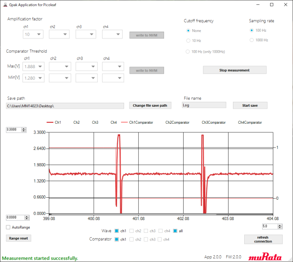
The EVK-v2 addresses these limitations by offering variable signal amplification and digital signal conversion for easy integration with microprocessors. Thanks to the use of the Renesas GreenPAK IC, the board can connect up to 4 sensors simultaneously. Key features of the EVK-v2 include:

  • Graphical User Interface (GUI):
    • Displays real-time analog signal output.
    • Enables dynamic switching of the amplification rate.
    • Allows quick adjustment of on/off detection thresholds.
Murata Unveils New EVK-v2 Evaluation Board for Picoleaf Piezoelectric Film Sensor

This streamlined design reduces the complexity of evaluating Picoleaf, accelerating product development cycles.


Technical Specifications of the EVK-v2

ParameterDetails
Evaluation Board NameEVK-v2 (Product No.: KT-DKPS017)
Integrated ICRenesas GreenPAK SLG47004V*
GUI AvailabilityDedicated GUI included
Channels SupportedUp to 4 simultaneous channels
InterfaceUSB Type-C
Noise FilteringYes

(*Product number subject to change without notice)


Conclusion

With its enhanced flexibility and ease of use, Murata’s EVK-v2 evaluation board offers developers an efficient way to leverage the capabilities of Picoleaf sensors. The ability to dynamically adjust signal amplification and thresholds through an intuitive GUI simplifies the evaluation process, enabling faster product development.

For more information, please visit www.murata.com.

Fujitsu Unveils AI Computing Broker to Optimize GPU Efficiency Amid Global Shortages

0

Fujitsu has introduced AI computing broker middleware designed to boost GPU efficiency and alleviate the challenges posed by the global GPU shortage. The new technology incorporates Fujitsu’s adaptive GPU allocator, a proprietary system that dynamically distributes GPU resources for real-time, high-efficiency AI processing. By combining this with various AI optimization methods, the solution addresses the growing demand for AI workloads while managing power consumption effectively.


Pilot Success and Industry Adoption

TRADOM Inc. will roll out solutions based on Fujitsu’s AI computing broker starting October 2024. Additionally, SAKURA internet Inc. has initiated a feasibility study to integrate this technology into its data center operations.

Earlier trials—conducted since May 2024 with companies like AWL Inc., Xtreme-D Inc., and Morgenrot Inc.—showed significant improvements. The trials revealed up to 2.25x better GPU processing performance and a substantial increase in the number of AI tasks that could be run simultaneously across multiple servers and cloud environments.

The AI computing broker will be available to customers in Japan starting October 22, 2024, followed by a global rollout.


Tackling AI-Driven GPU Demand and Energy Challenges

The rapid growth of AI technologies, including generative AI, has driven an unprecedented need for GPUs, which are more suitable for AI workloads than CPUs. Global demand for AI hardware is projected to grow 20 times by 2030, leading to increased power consumption. Current estimates suggest that data centers could account for 10% of the world’s electricity usage by 2030.

To address this issue, Fujitsu developed adaptive GPU allocation technology in November 2023. This technology optimizes CPU and GPU use by prioritizing processes with higher efficiency, even during active GPU workloads. This real-time optimization aims to increase computational output while reducing energy consumption.


AI Computing Broker: Key Features and Performance

The AI computing broker middleware integrates GPU allocation with advanced AI optimization techniques. It offers dynamic resource allocation at the GPU level rather than assigning resources on a per-job basis, resulting in higher availability and performance. The middleware’s memory management system also allows users to run multiple AI processes simultaneously without worrying about memory constraints, supporting workloads up to five times the physical GPU capacity (up to 150GB).

In trials, the technology improved GPU processing times by 2.25x compared to conventional methods. It also enabled parallel AI model training and testing, reducing overall execution time by nearly 10%.


Industry Endorsements and Use Cases

  • TRADOM Inc.:
    “Our pilot with Fujitsu’s AI computing broker streamlined GPU allocation, significantly accelerating the development of our AI models for foreign exchange risk management,” said Junichi Kayamoto, Chief Data Science Officer at TRADOM. “This collaboration is essential for expanding our solutions and driving innovation in the FinTech sector.”
  • SAKURA internet Inc.:
    Ken Wakishita, Senior Director of SAKURA Internet Research Center, noted: “The AI computing broker improved GPU efficiency within our cloud business, enabling broader access to GPU resources. We look forward to integrating this technology to meet growing market demand.”
  • AWL Inc.:
    Hiroshi Fujimura, R&D General Manager at AWL, commented: “Optimizing GPU costs for parallel model training is critical for our AI-powered retail solutions. Fujitsu’s broker technology improved GPU utilization, helping us meet client demands efficiently.”
  • Xtreme-D Inc.:
    Naoki Shibata, CEO and CTO, shared: “Our cloud platform Raplase caters to AI and HPC clients who need to optimize performance. Fujitsu’s AI computing broker addresses the challenge of efficient GPU utilization, and we are working closely with them to integrate it into our services.”
  • Morgenrot Inc.:
    Masamichi Nakamura, COO, and Hisashi Ito, CTO, highlighted: “Our decentralized approach to cloud computing benefits from Fujitsu’s technology. During trials, we achieved faster execution by sharing GPU resources between jobs, unlocking new possibilities for simultaneous AI workloads. We look forward to further collaboration with Fujitsu.”

Future Expansion and Application

Fujitsu plans to extend the AI computing broker’s functionality to multiple GPUs across servers, anticipating broader use in large-scale computing environments. As part of its ongoing efforts, Fujitsu aims to tackle challenges related to GPU availability and energy efficiency, enabling sustainable AI development and boosting productivity for businesses.

For more information, visit www.fujitsu.com.

STMicroelectronics Introduces Hybrid Page EEPROM for Low-Power, Compact Applications

STMicroelectronics has unveiled its new Page EEPROM, a hybrid memory solution that combines the power efficiency and durability of EEPROM with the speed and capacity of Flash memory. This innovative memory technology is designed for applications with extreme size and power constraints, making it ideal for wearables, IoT devices, and other embedded systems.


Meeting Evolving Storage Demands in Embedded Systems

As embedded applications become more sophisticated and require greater data storage—particularly for edge AI algorithms—ST’s Page EEPROM offers a solution that enhances efficiency without compromising on size. Behind-the-ear hearing aids are one such example, where the memory helps reduce the bill of materials, leading to sleeker, more comfortable designs.

Page EEPROM is also well-suited for healthcare devices, asset tracking systems, e-bikes, and other consumer or industrial products. “The evolution of the intelligent edge is driving new demands for memory storage density, performance, and power efficiency,” explained Philippe Ganivet, product line manager at STMicroelectronics. “Our Page EEPROM provides ultra-low power performance, making it an excellent companion for microcontrollers in battery-operated IoT modules.”


Performance Validation and Use Cases

BitFlip Engineering, an early adopter of ST’s Page EEPROM, has already integrated the memory into its GPS trackers and IoT devices. “This memory allowed us to meet ambitious performance targets,” said Patrick Kusbel, owner of BitFlip Engineering. “The M95P series delivers exceptional performance—up to 50 times faster, consuming just a tenth of the power, and offering five times the reliability compared to previous solutions.” With 500,000 write cycles compared to the industry-standard 100,000, it is a significant improvement over conventional EEPROMs.


Features of the Page EEPROM Family

The Page EEPROM family is available in 8Mbit, 16Mbit, and 32Mbit densities, offering greater storage capacity than traditional EEPROMs. It supports byte-level writes for efficient data logging, as well as page/sector/block erase operations for faster firmware updates via over-the-air (OTA) programming. With buffer loading functionality, multiple pages can be programmed simultaneously, reducing software installation time during production.

The memory’s data-read speed reaches 320 Mbit/s, approximately 16 times faster than standard EEPROM. Additionally, write-cycle endurance of 500,000 cycles ensures long-term reliability. To address power concerns, the device uses peak-current control, minimizing noise and extending battery life. It also includes a deep power-down mode with a quick wake-up function, drawing less than 1µA of current.


Built for Long-Term Reliability

Page EEPROM ensures 100-year data retention, meeting the needs of products requiring long-lasting performance. It is also part of ST’s 10-year product longevity program, which guarantees long-term availability for customers.


Development Tools and Availability

For developers interested in adopting this technology, ST offers the X-NUCLEO-PGEEZ1 expansion board and X-CUBE-EEPRMA1 software package. These tools allow users to explore the hybrid memory architecture and quickly build proof-of-concept applications. The software package includes a demonstration to facilitate rapid testing and integration.

The M95P08 (8Mbit), M95P16 (16Mbit), and M95P32 (32Mbit) Page EEPROMs are now in production, with the M95P08 priced from $0.50. The X-NUCLEO-PGEEZ1 expansion board is available through the eSTore for $40.00.

For more information, visit www.st.com/page-eeprom.

Honeywell and Google Cloud Join Forces to Accelerate AI-Driven Industrial Operations

0

Honeywell and Google Cloud have announced a unique collaboration aimed at enhancing industrial operations through the integration of artificial intelligence (AI), connecting assets, people, and processes to support safer and more autonomous operations across industries.

This partnership leverages Google Cloud’s Gemini AI models on Vertex AI, known for their multimodal and natural language capabilities, alongside the vast data collected on Honeywell Forge, a leading Internet of Things (IoT) platform for industrial applications. The integration will deliver clear, actionable insights across various use cases, helping Honeywell’s customers reduce maintenance costs, improve productivity, and upskill workers. Honeywell plans to roll out the first AI-enabled solutions in 2025.


Driving Smarter and Autonomous Operations

“The journey to autonomy requires assets to perform better, people to work more intelligently, and processes to operate more efficiently,” said Vimal Kapur, Chairman and CEO of Honeywell. “By combining Google Cloud’s advanced AI technology with the industrial knowledge and data within Honeywell Forge, we can provide powerful insights that bridge the gap between the physical and digital worlds—accelerating autonomous operations, a key element of Honeywell’s growth strategy.”

According to Thomas Kurian, CEO of Google Cloud, the collaboration “marks a major advancement in bringing AI’s transformative potential to industrial settings. With Gemini on Vertex AI and Honeywell’s industrial expertise, we are creating new opportunities for process optimization, workforce empowerment, and improved business outcomes.”


AI-Driven Solutions for the Industrial Sector

The industrial sector is currently grappling with labor shortages and skills gaps, exacerbated by the retirement of baby boomers. While 82% of Industrial AI leaders identify their companies as early adopters of AI, only 17% have fully implemented AI strategies, according to Honeywell’s 2024 Industrial AI Insights Report. The collaboration aims to increase AI adoption by augmenting operations and workforce performance, enabling organizations to harness automation for growth without reducing jobs.

Purpose-Built AI Agents

  • Honeywell and Google Cloud will develop AI agents, powered by Vertex AI Search, to support engineering tasks, automate workflows, and shorten project design cycles. This allows engineers to shift their focus towards innovation and customer satisfaction.
  • Specialized AI agents will also utilize large language models (LLMs) to assist technicians with maintenance tasks by providing real-time answers to questions such as, “How did the system perform overnight?” or “How do I replace this module?” Gemini’s multimodal capabilities will enable these agents to interpret images, videos, text, and sensor data, providing deeper insights beyond simple queries.

Improving Cybersecurity and Edge Device Capabilities

The partnership will also strengthen cybersecurity by integrating Google Threat Intelligence, including insights from Mandiant, with Honeywell’s security solutions such as GARD Threat Intelligence and Secure Media Exchange (SMX). This collaboration will enhance threat detection and protection for critical infrastructure.

On-the-Edge AI Innovations

Honeywell plans to explore the use of Google’s Gemini Nano model to enhance its edge AI devices. These improvements will support multiple use cases—ranging from advanced scanning performance to voice-guided workflows, operational monitoring, and alarm handling—without needing cloud connectivity. Honeywell anticipates that these new intelligent devices will be part of future product announcements, marking a significant step toward autonomous operations.


Alignment with Key Market Trends

By integrating Google Cloud’s technology, Honeywell reinforces its alignment with three key market trends: automation, increased productivity, and workforce empowerment. The partnership emphasizes AI’s role not only in enhancing operational efficiency but also in helping companies adapt to emerging challenges and drive sustainable growth.

This collaboration lays the foundation for next-generation industrial solutions, combining AI-powered insights with Honeywell’s expertise in operational technology, positioning both companies to shape the future of autonomous and connected industries.

Anritsu Selected by Sunnyverse for Wireless Performance Testing of XR Devices

Anritsu Corporation has announced that Zhejiang Sunnyverse Technology Co., Ltd., a leading developer of Extended Reality (XR) devices, has chosen Anritsu’s testing solutions to evaluate the RF TRx performance of the wireless LAN (WLAN) and Bluetooth technologies integrated into their devices.


The Need for Fast, Reliable Wireless Connectivity in XR Devices

The market for XR technologies, including Augmented Reality (AR) and Virtual Reality (VR), is expanding rapidly across industries like entertainment and education. As these devices rely on high-speed data transfer and low latency to provide immersive user experiences, wireless communication performance is critical for seamless operation. To meet these needs, Sunnyverse sought advanced tools to assess the RF transmission and reception (TRx) performance of their WLAN and Bluetooth technologies, which are key to ensuring smooth data transfer.


Why Sunnyverse Chose Anritsu Solutions

Sunnyverse selected Anritsu’s MT8862A Wireless Connectivity Test Set and MT8852B Bluetooth Test Set for their ability to optimize RF performance measurements. These products streamline the testing process by offering clear, concise parameter settings, which accelerate time to market for Sunnyverse’s XR devices.

MT8862A Wireless Connectivity Test Set

  • Supports RF TRx measurements for WLAN standards, including IEEE 802.11a/b/g/n/ac/ax/be across the 2.4 GHz, 5 GHz, and 6 GHz bands.
  • Features 2×2 MIMO Rx sensitivity and Tx power measurement capabilities, crucial for WLAN performance optimization.

MT8852B Bluetooth Test Set

  • Certified by the Bluetooth SIG for RF performance evaluations.
  • Offers 2 Mbps Low-Energy PHY (2LE) and Bluetooth Long-Range (BLR) testing options, ideal for low-power and extended-range applications.

Future XR Developments and the Role of 5G

As the XR market evolves, devices will increasingly incorporate 5G technology to achieve higher bandwidth and lower latency. In addition to its WLAN and Bluetooth solutions, Anritsu is committed to offering comprehensive 5G testing tools, ensuring that XR devices meet future connectivity demands and deliver superior user experiences.


Explore Anritsu’s Solutions

To learn more about how wireless connectivity supports AR/VR technologies, explore Anritsu’s case study interview: “Profound Contents to Be Enabled by Wireless Connectivity of AR/VR” (PDF).

For product details:

  • MT8862A Wireless Connectivity Test Set: WLAN testing across multiple frequency bands and standards.
  • MT8852B Bluetooth Test Set: Advanced Bluetooth performance measurements.

Visit www.anritsu.com for more information.


With these cutting-edge testing tools, Anritsu is helping Sunnyverse and other manufacturers enhance wireless performance, streamline development, and ensure XR devices meet growing industry demands.